Machine Parts For Reuse Newsgroup Discussion Forum > Large Size Parts
> Dsp development board DSP2407 TMS320LF2407A cpld
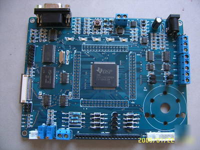
Dsp development board DSP2407 TMS320LF2407A cpld
DSP development board, DSP2407 development board, TMS320LF2407 development board
The development kit is based on the TMS320LF2407A study of DSP development platform. TMS320LF2407A with a large number of peripheral resources, respectively, two of the event management module EVA, EVB; two 16bit counter the overall situation; 8-channel pulse width modulated adjustable PWM; three external events to capture the regular sampling unit; synchronized 16-channel high-performance 10bit ADC, the conversion rate of 500ns; Serial asynchronous communication interface (SCI); synchronous serial peripheral interface (SPI); CAN bus 2.0 interface.
Full advantage of this package to provide a large number of peripherals TMS320LF2407A resources, together with detailed information and the use of a large number of instances (all provided by source), making this product as a learning DSP system of choice for developers, can also be used directly for the number of embedded control systems, reduce costs and quickly into the market.
TMS320LF2407A, a maximum operating frequency of 40MHZ;-chip built-in 32K * 16 bit FLASH, users can be stored procedures, FLASH can be encrypted; built-in 2.5K * 16 bit DARAM, can be configured into a data area and procedures for the district.
DSP chip to expand 64K * 16-bit IS61LV6416 SRAM, can be used as a data area (32K), the procedure can also be used as areas (32K) to use.
expanded 2Kb serial EEPROM (AT24C02 chip), can be used for data transmission and storage.
DSP generated using both the PWM dead-band signal, the use of transistor-driven, micro DC motor can be controlled positive.
board provides a standard 6-pin stepper motor interface, you can access a variety of micro-stepping motor. By modifying the procedures to control the motor.
board to provide a 20-pin LCD graphical interface, users can access commonly used Chinese font with LCD 12864.
board to provide a 16-pin LCD interface characters, user-friendly access of small character LCD, such as liquid crystal, such as 1602.
DA in part with the use of TI's 4-way serial control of 8-digit A / D converter chip TLC5620C.
2407A-built 16-channel 10-bit AD converter, the development board through the isolation amplifier extends only two-channel (channel 0 and channel 8), the user can be expanded to 16.
board in the development of CAN bus transceiver is used in models PCA82C250. CANRX it into CANTX and CANH and CANL transmission in the CAN bus.
SCI serial communication interface
TMS320LF2407A embedded chip serial communication interface (SCI) module. RS232 interface chip on the board using the MAX232, the DB9 standard socket interface, user-friendly serial cable connections.
SPI Serial Peripheral Interface
TMS320LF2407A chip embedded hardware serial peripheral interface (SPI). Development board using the SPI interface (IO mode) control of a Seven-Segment LED; other DSP through the SPI interface and D / A converter connected to TLV5620 chip.
board to provide a free button and the DSP-IO port (IOPB7) is directly linked to the realization of a simple man-machine operation, such as through manual buttons on the control board LED, etc. 4.
extended interruption of the development of on-board input interface, in which the DSP interface input termination XINT2 there is a small button EXINT, as long as the user pressed the button, EXINT pin on the input of a low-level, in the corresponding software installed on the disruption can occur.
reset circuit we use a special reset chip SP708R, a DSP chip to ensure reliable reset, and to provide a manual reset button, user-friendly for program debugging.
In order to facilitate the development of the user after the expansion, we will be the main pin TMS320LF2407A chip interface leads passed.
development board used is a 5V power input, not only by the switching regulator 5V/1A external power supply, or directly through the USB port power supply, user-friendly.
standard 14-pin JTAG interface (6 feet the first of which is empty), you can connect a variety of TI's DSP Emulator. Debugging and procedures is essential programmer interface.
[Code and related experiments]
TMS320LF2407A have four general-purpose timer, the program mainly to operate a general-purpose timer to 1ms interrupt generated 1, drive the development of the D1 board constantly blinking light-emitting diodes. Users can modify the program to enable timer 2 control other light-emitting diodes.
2, disruption of the importation of the experiment
Board on the expansion interface interrupt input, which input termination EXINT a small button, as long as the user press the small button, EXINT appear low on the pin. Load after interruption of program to run, press the button EXINT generate external interrupt, it can be seen on the board four to speed up the flashing light-emitting diodes.
Board there are D1, D2, D3, D4 four light-emitting diode, LED program to run after the load, D1, D2, D3, D4 followed by light-emitting, and then light the whole time; procedures to keep the cycle running.
4, button LED control experiment
Development board provides a micro-keys KEY, the procedure can be controlled through the output device. Our process is button control board on the four LED, the experiment is: after the program is running, press the KEY button, LED1 flashes continuously; according to the second, it is constantly flashing LED2; by the third, it is constantly flashing LED3 ; by the fourth, it is constantly flashing LED4; by the Fifth, it is followed by LED1-LED4 blinking cycle; KEY button and then repeat the above phenomenon.
5, the experimental data RAM read and write
The development of the widening of an outside board 64K * 16 bit SRAM, through the definition of logical combinations of its RAM and procedures for data RAM, of which the low 32K of address space is defined as data space. After loading the program to run at full speed, if the development of on-board four of the D1 to D4 rapid blinking LED on the external data RAM space is working.
6, the experimental procedure to read and write RAM
Procedures for the external RAM memory space to occupy the high 32K address space. External RAM test procedure can only be carried out through the CCS, in the hardware simulation environment, open the CCS software MEMORY Enter starting address and length, fill in the VALUE column of data (such as 0X5555), and then PROGRAM; through the View Memory See the procedures of this RAM address space has been changed into the corresponding data (for example, 0X5555), if the procedure has been changed from that RAM is no problem.
7, EEPROM read and write outside the extended experimental
Expansion of the development of a 2Kb on-board serial EEPROM chip (AT24C02), users can be used to store data. In this experiment carried out through the DSP to read and write data operation, EEPROM load process to run through into the WATCH window can be observed and read out the data, then compare the data and write the data read out.
8, SCI serial communication experiment
Development board using the straight-through DB9 serial cable to the DSP and the PC's serial port to link up. First of all open debug serial PC-assistant software, using default settings and select 16-band receive and transmit; load operation after SCI, in the serial port reception assistant continuously receiving display data and 16-band 57, the user can assistant send data through serial port (such as 16 hex 75) to the development board, in the WATCH window view of the data received. SCI is a full duplex serial communication.
9, SPI Bus Interface Experiment
SPI bus system is a high-speed synchronous serial interface, it can be a microcontroller with a wide range of peripherals to the serial communication means to exchange information. SPI control this process through the digital board on display. After running the program can be seen on the LED board from'0 'to' F 'cycle revealed that at the same time 4 LED flashes continuously.
The development board through the expansion of the isolation amplifier 2407A-chip AD converter channel 0 and channel 8, the user can enter in the AD terminal on the external ADIN0 and a voltage ADIN8 (Note: the external input voltage must be less than 3.3V to avoid damage to the device), and then run the AD process, set breakpoints, and debug-> Animate monitoring data in the WATCH window so you can view the tracking data AD0 and AD8.
2407A through SPI and TLC5620 chip DA converter connected, the program is running, the user can be measured oscilloscope DA1 and DA2 output triangular wave with a multimeter to measure DA3 and DA4 were 1.2V and 0.8V output voltage.
12, DA-AD Joint Experiment
This experiment by two DA output voltage as input signal AD (to be short-J23 pin 1,2 then pin 3,4 can be shorted, development board has been shorted by default good). Joint DA-AD to run the experimental procedure, in the WATCH window AD_SIG0 and input variables AD_SIG8 collected to see the way these two voltage values.
13, CAN bus communication experiment
CAN bus debug external CAN device needs, in the absence of external CAN equipment, the procedures for the use of self-test mode of CAN communications, CAN receive interrupt the use of information. CAN running process, users can see WATCH window ReceiveData the value of variables (8).
14, the experimental character liquid crystal display
This procedure is compatible with Driver IC HD44780, KS0066, SPLC780 characters, such as liquid crystal (such as commonly used in 1602), the LCD 1602 into the J1 socket on board, loader running, in 1602 on the LCD to display "www.00IC . com "and other words.
15, Chinese liquid crystal display experiments
20-pin board on the LCD interface, can take over 12,864 Chinese font with LCD (Driver IC for ST7920); run the program, the LCD display for some characters in the font.
16, DC motor control experiment
This procedure aimed at micro DC motor. Two of the PWM dead-band signal generated directly from the DSP, motor drives using four NPN transistor, positive control. After running the program can see the motor to start rotating, procedures in the frequency of the PWM is 1KHZ, the user can modify the parameters XPWM can control motor speed and direction.
17, stepper motor control experiment
Board to provide the standard 6-cell stepper motor interface, which can be accessed by micro-stepper motor. Stepper motor control program is running, you can control the operation of stepper motor and at the same time can see the board on the four light-emitting diode LED flashes followed by the cycle.
18, interrupt vector programmer experiment
Simulation debugger users, it is necessary to state simulation programmer interrupt vector. Our products in the factory simulation programmer interrupt status to the scale, user-friendly learning directly into the debug state. First of all, J9 board will develop a short circuit risk VCCP jump jumper +5 V, that is, the left legs 1,2; then good simulation and development board, open the CCS programmer's "cloud" button interrupt programmer configured to scale ( We have detailed the Notes) and set the programmer options and the path, click the Execute button programmer. Programmer can enter the CCS after the completion of debugging.
19, FLASH programmer (curing process) Experimental
Users to debug the compiler to prepare the success of the procedure, the need for curing to FLASH in order to operate independently from the simulator, which is curing process on the need for the programmer of the FLASH. We detail the steps the programmer, and a specific example to illustrate the experiment to ensure that future users can be a good programmer debug compile their own procedures.
Note: All of the above experimental procedures to compile all of the CCS3.3 recommend that users install CCS3.3, because the programmer CCS3.3 do not need to install plug-ins, CCS3.1 previous programmer required to install plug-ins; In addition, we The XDS510 emulator TDS510 and the full support of all CCS3.3, for the user to choose , all code using C language, and the Notes to ensure that beginners Quick Start!
[Supporting information and software]
1, all instances of the integrity of the process engineering documents, all to provide the source code;
2, a complete schematic diagram (pdf format), a number of practical technologies to grasp the specific application;
3, online download of the method and tool for curing the user's own procedures;
4, user's manual: a very detailed and allows you to quickly enter the door to the development and application of DSP;
5, the chip manual: the development of chip-chip on-board all the information;
6, the original TI DSP development environment CCS3.3, all programs are compiled under the CCS3.3;
7, matrix extraction software
8, serial debugging software
9, presented information on other DSP-related learning.
[Application of information given]
1, to send TCP / IP protocol volumes: Volume 1, Volume 2, Volume 3
2, sent to USB1.1 protocol specification documents
3, sent to U disk system documentation
4, sent to FAT16, FAT32 system documentation
5, to send SCSI command set documentation
6, sent to the development of other related documentation
1, DSP system development study
2, industrial automation control
4, digital filtering, vibration analysis
6, variable frequency control
1, testing a piece of good development board TMS320LF2407A
2, Direct Connect a serial line
3, USB power supply line 1
6, a supporting CD-ROM (DVD)
7, presented "DSP Technology" 3G video more
8, a warranty card (the only serial number of certificate)